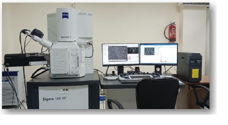
The SIGMA 500VP Field Emission Scanning Electron Microscope (FE-SEM), equipped with Energy Dispersive X-ray Spectroscopy (EDS) and Electron Backscatter Diffraction (EBSD) sensors, is known for its advanced capabilities in imaging and material analysis. Below are the major specifications for this sophisticated instrument:
SIGMA 500VP FE-SEM Major Specifications
General Specifications:
- Model: SIGMA 500VP
- Electron Source: Field Emission Gun (FEG)
- Vacuum Modes: High vacuum, variable pressure (VP)
Imaging Performance:
- Resolution:
- High Vacuum Mode: 1.0 nm at 15 kV, 1.7 nm at 1 kV
- Variable Pressure Mode: 1.4 nm at 20 kV
- Magnification: 12x to 2,000,000x (depends on configuration and sample)
- Accelerating Voltage: 0.02 kV to 30 kV
- Probe Current: 3 pA to 20 nA
Detectors:
- Secondary Electron (SE) Detector: Provides high-resolution surface images.
- Backscattered Electron (BSE) Detector: Enables compositional contrast imaging.
- In-lens SE Detector: Offers enhanced resolution and surface detail contrast.
- Variable Pressure SE Detector (VPSE): For imaging in variable pressure mode.
Analytical Capabilities:
- Energy Dispersive X-ray Spectroscopy (EDS):
- Elemental Detection Range: From boron (B) to uranium (U)
- Mapping Capabilities: Elemental mapping and line scan analysis
- Electron Backscatter Diffraction (EBSD):
- Crystallographic Analysis: Grain orientation, phase identification, and texture analysis
- Resolution: Down to nanometer scale for EBSD mapping
Stage and Sample Handling:
- Stage: 5-axis motorized stage
- X/Y Travel Range: 100 mm
- Z Travel Range: 50 mm
- Tilt: -3° to +70°
- Rotation: 360° continuous
- Sample Size: Up to 200 mm diameter (depending on chamber size and configuration)
Software and Data Processing:
- Control Software: ZEISS SmartSEM
- EDS Software: Integrated with EDS analysis software for elemental identification and quantification
- EBSD Software: Integrated with EBSD analysis software for crystallographic analysis
Additional Features:
- Charge Compensation: Available in VP mode for imaging non-conductive samples
- Chamber Size: Spacious chamber to accommodate large samples and multiple detectors
- User Interface: Intuitive interface for ease of use and efficient workflow
These specifications highlight the capabilities of the SIGMA 500VP FE-SEM in providing high-resolution imaging and comprehensive material analysis through EDS and EBSD sensors. This makes it a versatile tool for researchers and engineers in various fields, including materials science, nanotechnology, electronics, and more.
The SIGMA 500VP Field Emission Scanning Electron Microscope (FE-SEM) with Energy Dispersive X-ray Spectroscopy (EDS) and Electron Backscatter Diffraction (EBSD) sensors offers extensive research potential across a variety of scientific and engineering disciplines. Here are some areas where the SIGMA 500VP can significantly impact research:
Materials Science
- Nanomaterials: High-resolution imaging and elemental analysis of nanoparticles, nanowires, and other nanostructures to study their properties, synthesis, and applications.
- Metallurgy: Analysis of metals and alloys to understand grain structure, phase composition, and defects, crucial for developing new materials and improving existing ones.
- Polymers: Investigating the morphology and composition of polymer blends, composites, and nanocomposites to enhance their mechanical and thermal properties.
Semiconductor and Electronics
- Failure Analysis: Identifying defects and failures in electronic components and semiconductor devices to improve reliability and performance.
- Process Development: Characterizing materials and processes in semiconductor manufacturing, including doping, layer deposition, and etching.
- Nanodevices: Imaging and analysis of nanoscale electronic and optoelectronic devices to optimize their design and functionality.
Life Sciences
- Biological Samples: Imaging biological specimens such as tissues, cells, and biomaterials to study their structure and composition.
- Biomineralization: Investigating the formation and composition of biominerals in organisms, which is important for understanding biological processes and developing biomimetic materials.
- Medical Implants: Analyzing the surface morphology and composition of medical implants to improve biocompatibility and performance.
Geosciences
- Mineralogy: Identifying and characterizing minerals in geological samples to understand their formation, distribution, and properties.
- Petrology: Studying the texture and composition of rocks to gain insights into geological processes such as magma crystallization and metamorphism.
- Paleontology: Examining the microstructure and composition of fossils to understand ancient life forms and environmental conditions.
Environmental Science
- Pollution Studies: Analyzing particulate matter and other environmental samples to identify sources of pollution and assess their impact on the environment.
- Soil and Sediment Analysis: Investigating the composition and structure of soils and sediments to understand their properties and interactions with contaminants.
- Biogeochemistry: Studying the distribution and cycling of elements in the environment to understand biogeochemical processes and their effects on ecosystems.
Forensic Science
- Trace Evidence Analysis: Examining trace evidence such as glass fragments, gunshot residue, and fibers to support criminal investigations.
- Toxicology: Analyzing biological samples for toxic elements and compounds to aid in forensic toxicology investigations.
- Document Examination: Investigating the composition of inks, papers, and other materials used in documents to detect forgeries and alterations.
Industrial Applications
- Quality Control: Ensuring the quality of materials and products in industries such as aerospace, automotive, and pharmaceuticals by analyzing their composition and structure.
- Failure Analysis: Investigating the causes of failure in industrial components and systems to improve their design and prevent future failures.
- Process Optimization: Monitoring and optimizing manufacturing processes by analyzing the materials and products at various stages of production.
Advancements in Analytical Techniques
- Method Development: Developing new analytical methods and techniques using the advanced capabilities of the SIGMA 500VP to push the boundaries of material analysis.
- Interdisciplinary Research: Combining imaging and analytical techniques to address complex research questions across multiple disciplines, such as combining materials science with biology or environmental science.
The SIGMA 500VP FE-SEM, with its high-resolution imaging and comprehensive analytical capabilities provided by EDS and EBSD sensors, is a powerful tool for researchers across a wide range of fields. Its versatility and advanced features enable detailed characterization and analysis of materials, leading to new insights and advancements in science and technology.